Electronics / PCB Quality Control
Inspection of solder joints, components, and defects on printed circuit boards.
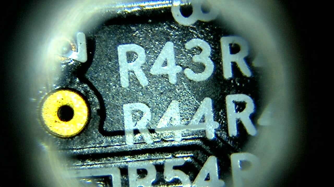
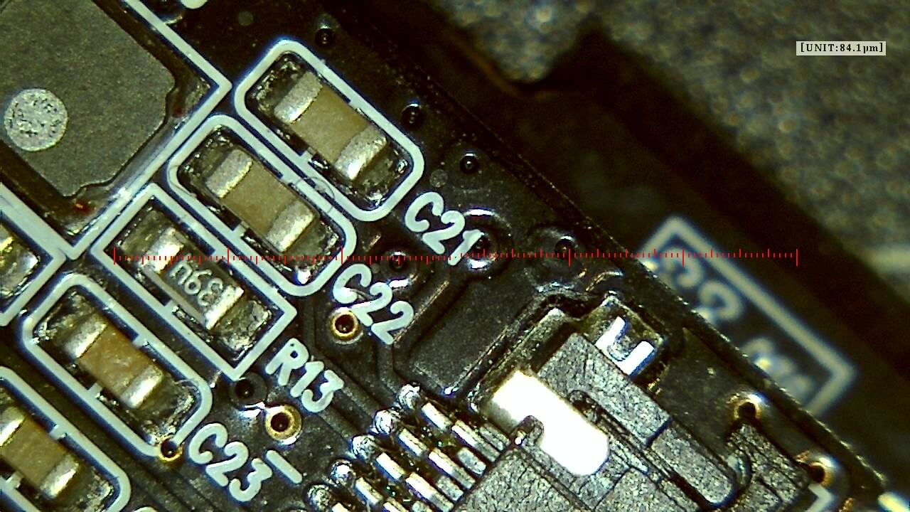
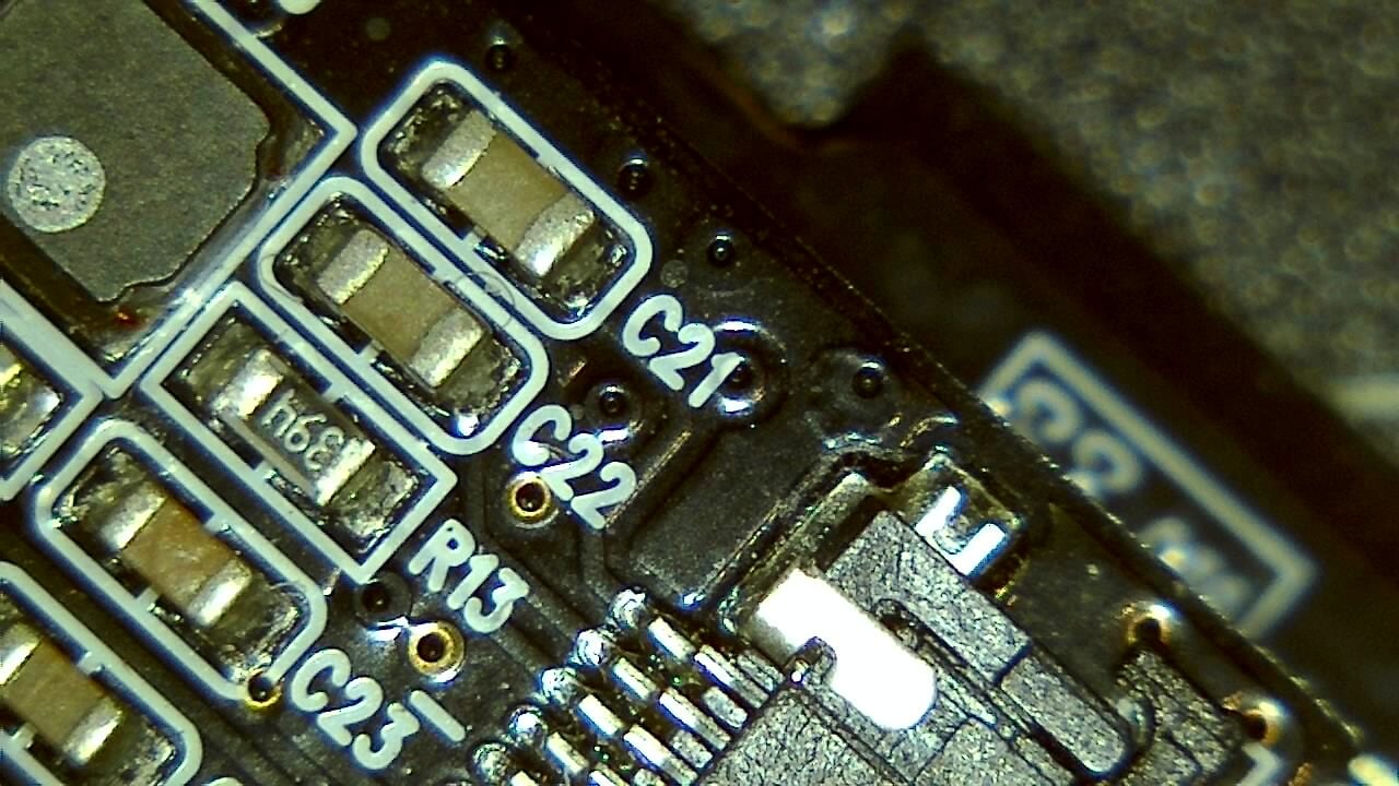
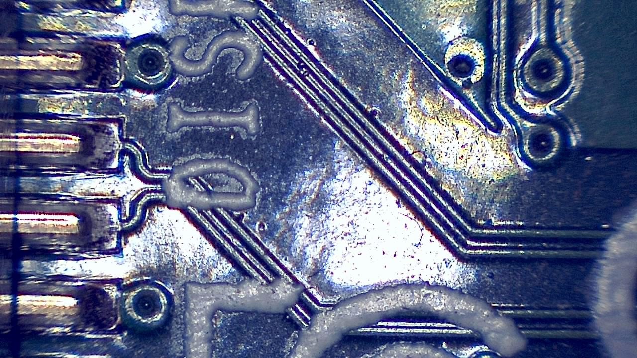
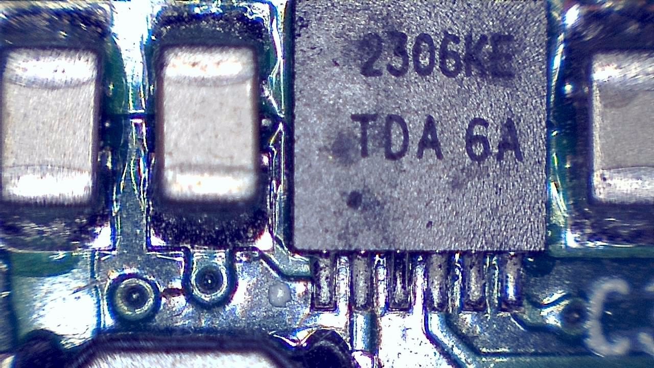
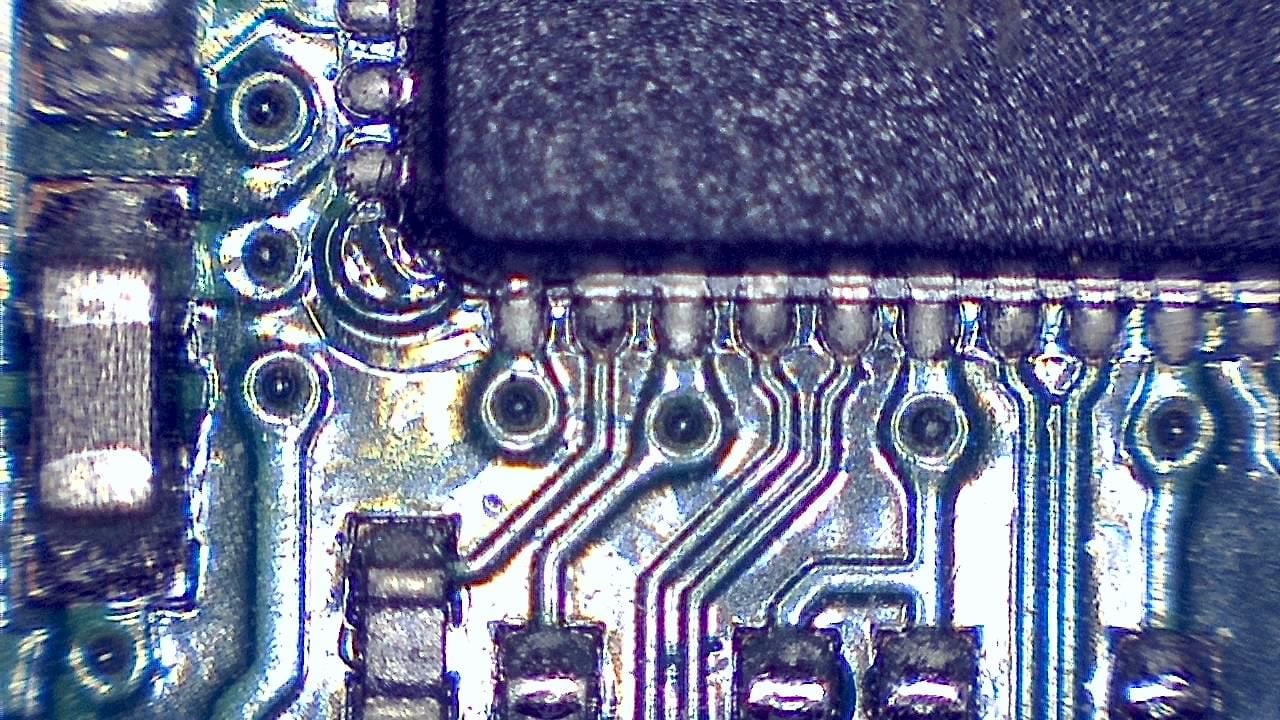
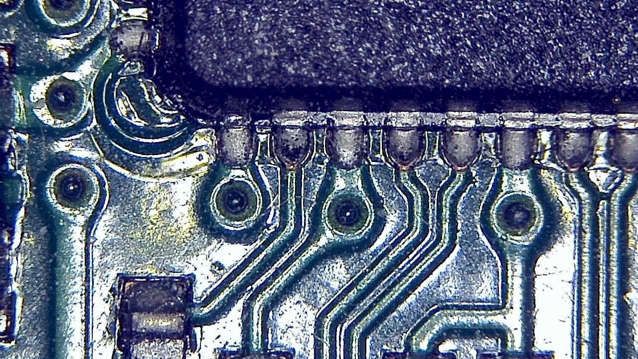
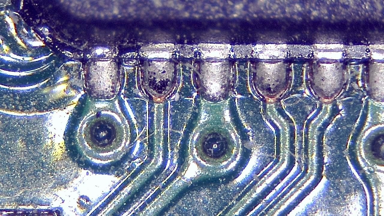
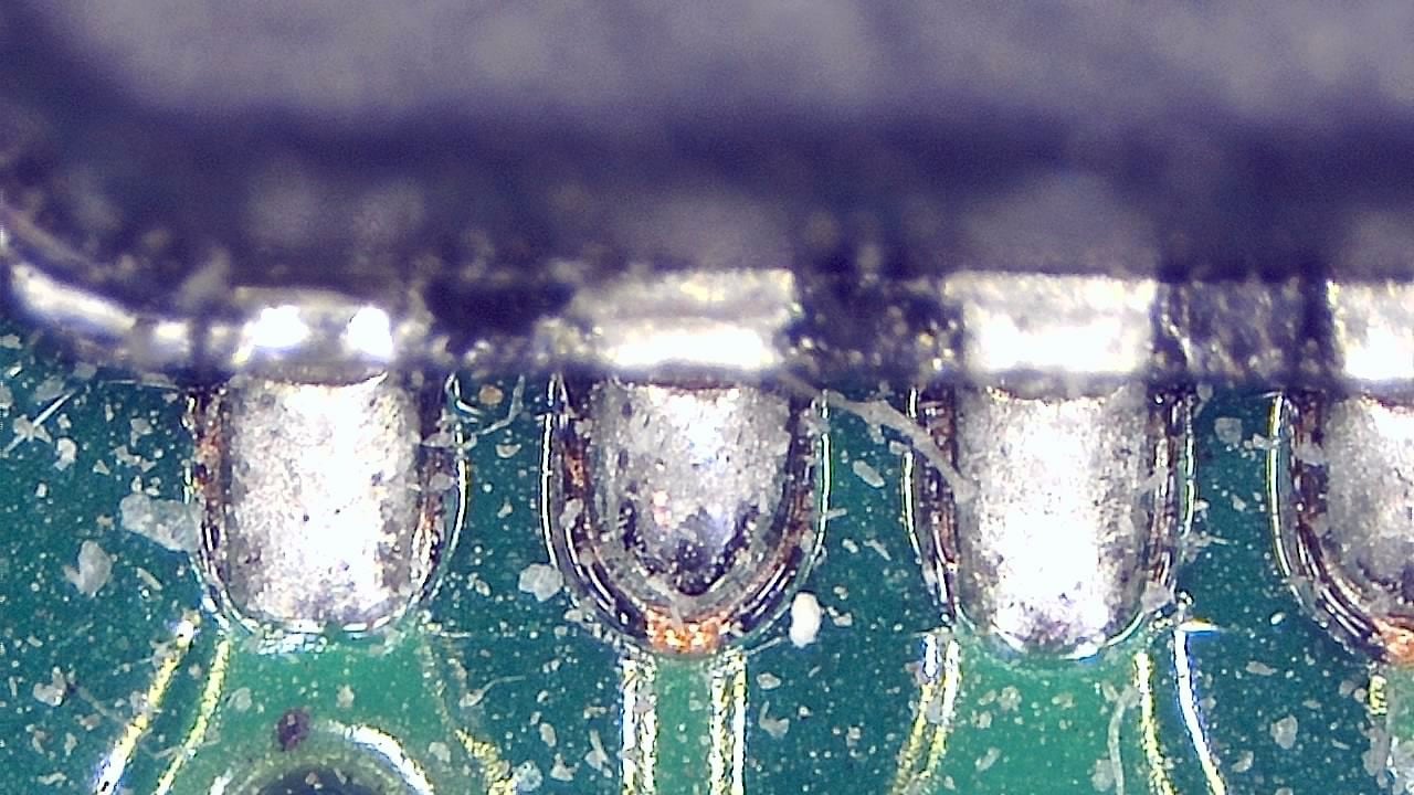
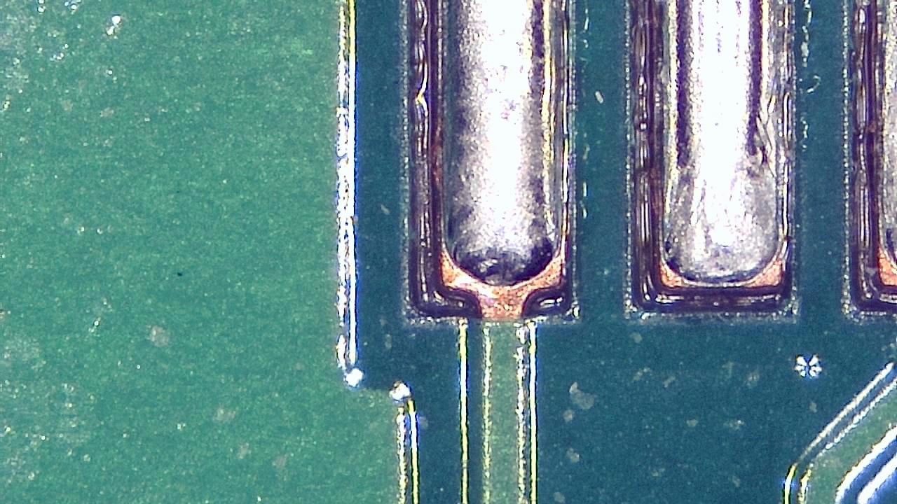
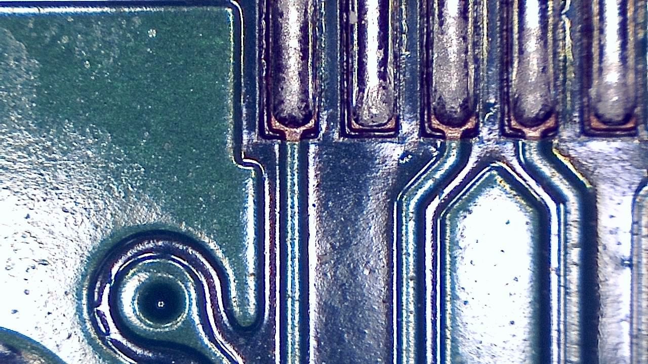
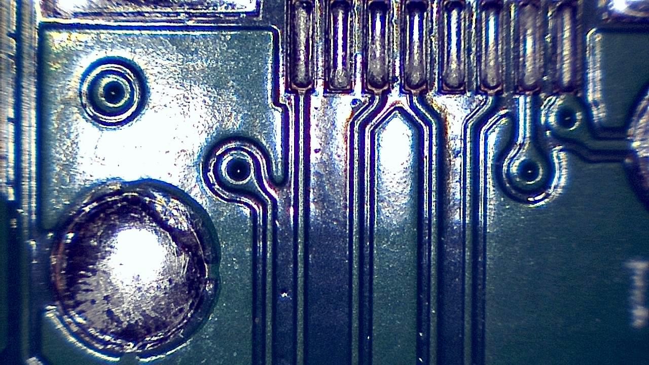
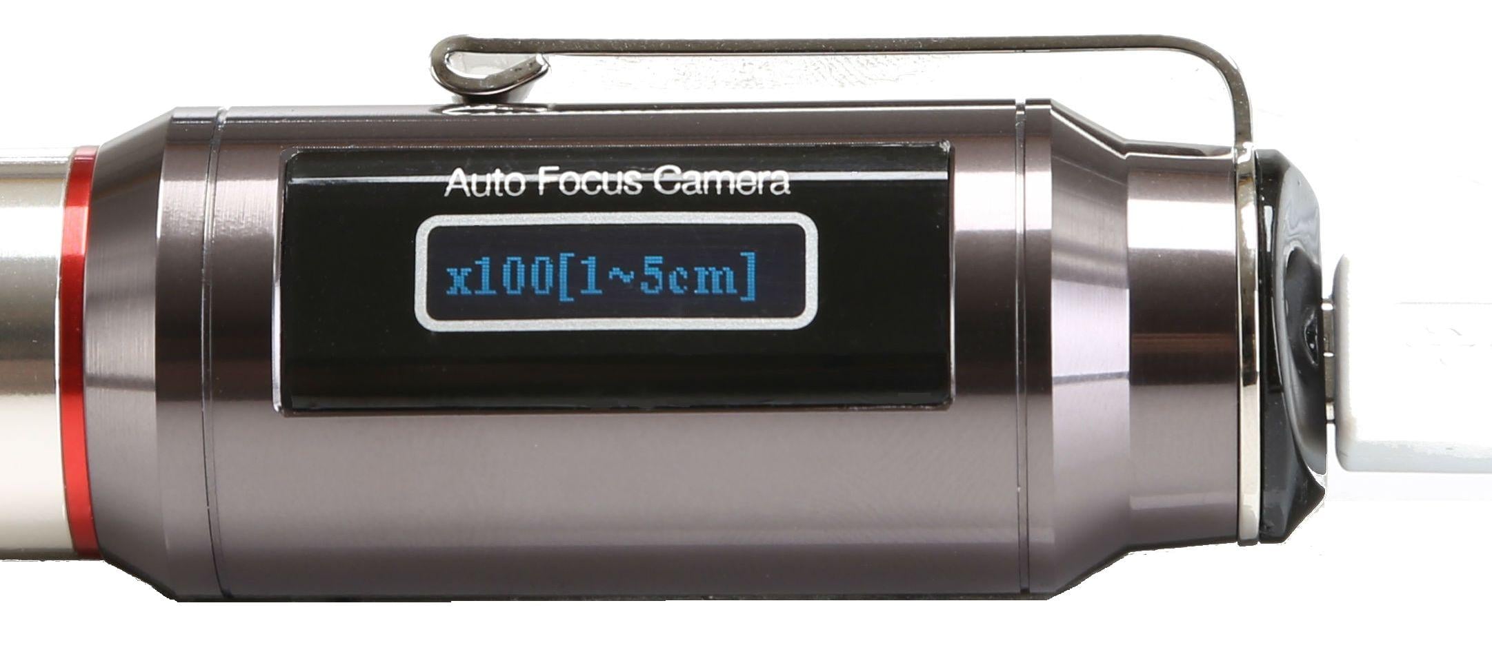
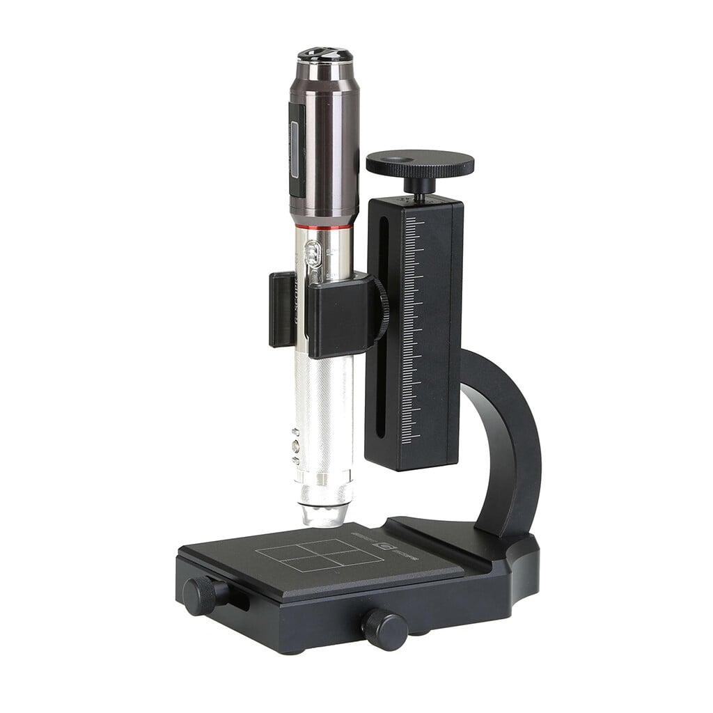
Component miniaturization demands high-precision visual inspection. Smart G-Scope enables engineers and quality technicians to inspect solder joints, traces, vias, and SMD components at magnification levels suitable for detecting microscopic defects.
It can help identify solder bridges, cracks, contamination, component misalignment, and wetting issues that may cause failures in production or in the field. Documenting defects supports traceability and continuous process improvement.
The device’s portability allows use both on production lines and in failure analysis labs, adapting to different industrial environments.
Key benefits
- Detection of microcracks, solder bridges, and solder balls
- Inspection of BGA, QFN, and micro-components
- Defect documentation for quality reports
- Failure analysis and lot traceability
- Usable in production and R&D labs
Image gallery

Click any image to enlarge
Practical examples
SMD soldering inspection
On an LED board production line, a quality technician uses Smart G-Scope to inspect samples from each lot, detecting solder bridges before boards move to the next process step.
Field-failure analysis
An engineer examines a returned board with intermittent failure. The microscope reveals a microcrack in a BGA joint caused by thermal stress, enabling a heatsink design correction.
Limitations & best practices
- Internal layer inspection requires X-ray or cross-section microscopy.
- Keep the work area clean to prevent cross-contamination.
- Calibrate magnification scaling for accurate measurements.
Interested in this use case?
Buy Smart G-Scope
Get the right kit for this application. Secure checkout and fast shipping.
Need help choosing? Tell us your workflow and we’ll recommend the best setup.
Related use cases
3D Printing
Surface quality control, layer defect detection, and material assessment for 3D-printed parts.
Jewelry/Watchmaking
Inspection of gemstones, settings, watch mechanisms, fine metalwork, and collectible coins for authentication and condition assessment.
Quality Control
Fast, accurate inspection of surfaces, parts, and assemblies to catch defects before they reach the customer.
Printing
Evaluate halftones, color registration, and print defects in detail for quality control in printing and packaging.
Food
Supports visual quality control of foods and raw materials through fast inspection and documentation.
Cosmetics
Visual inspection of textures, particles, and impurities for quality control and product development.
Textiles
Detect defects in fibers, weaves, and finishes for textile quality control.